Microscope Sub-micron Lithography
A conventional lab-grade microscope is utilized for photolithography, creating features down to the sub-micron scale.
Conventional microscopy and photolithography systems share numerous similarities; while the primary goal of a microscope is to magnify an image, a stepper, on the other hand, reduces it. These similarities can be harnessed to create a versatile, low-cost patterning system.
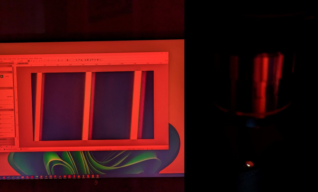
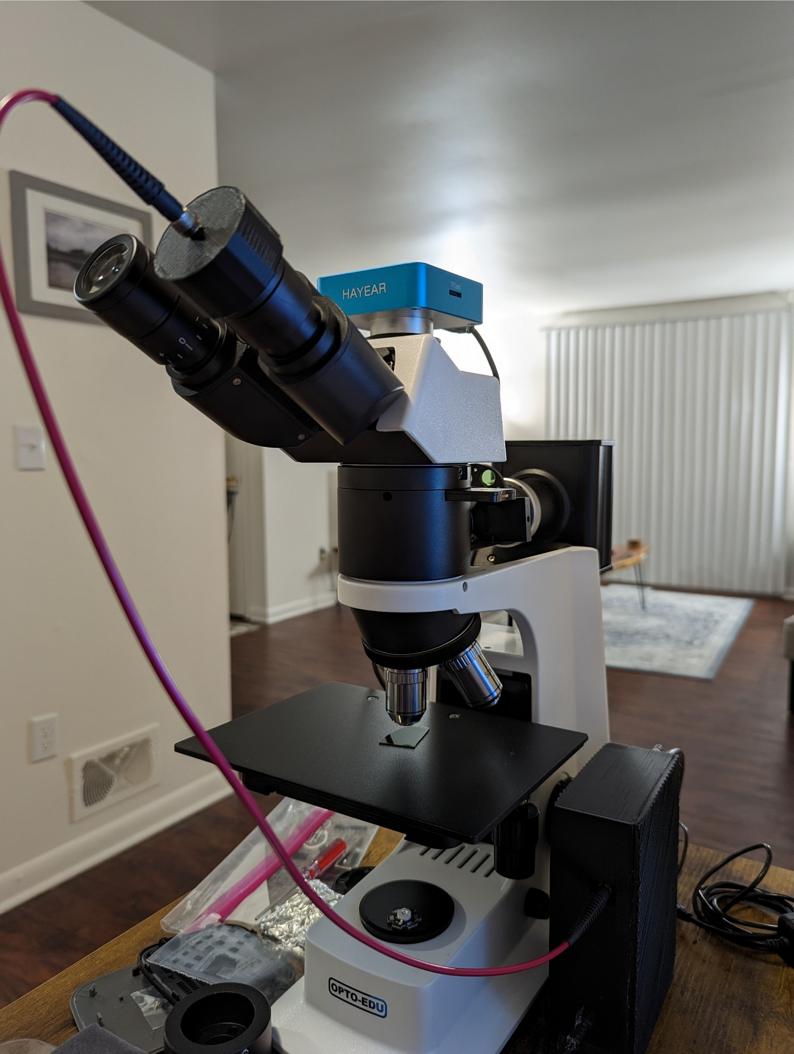
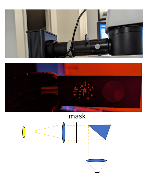
For optimal results, an infinity corrected microscope is employed to minimize focus distortions. Light from an LED passes through an aperture to a condenser lens, filter, polarizer, beam splitter, and finally the objective lens. Post the condenser lens, the beams are approximately parallel, allowing for a mask to be inserted into the beam path for patterning, although some diffraction from the mask is expected. The most practical point for mask insertion is identified at the polarizer's location. Eschewing cumbersome projector or other homebrew mask setups that yield poor resolution, a mylar photomask is utilized. Mylar photomasks can be affordably produced with a photoplotter by various external vendors, achieving feature sizes down to 7 microns. These masks can also be cut to shape and inserted into the spare slot on the polarization filter holder, secured with a piece of soda-lime glass and a 3D printed ring.
The LED on this microscope is instrumental for patterning. A conventional white LED is essentially a blue LED with a phosphor coating. By employing filters, the broader, longer wavelength emission from the phosphor can be used for alignment with the microscope camera while blocking the blue light. Once satisfied with the alignment, the filter can be swapped to allow the blue light at ~g-line 440 nm to expose the coated photoresist.
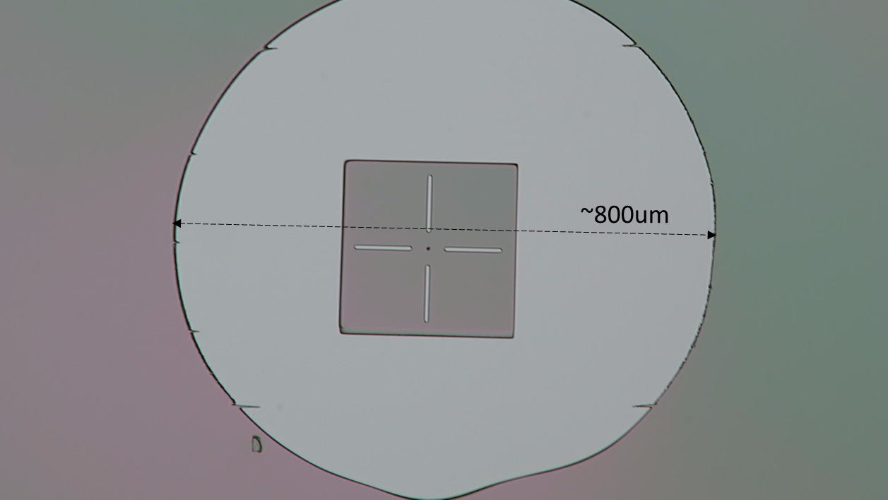
The drawback of utilizing a relatively inexpensive microscope is the high cost and bulkiness of good quality lenses, particularly large ones for lithography, limiting the exposure field size—in this case, a circle of ~800 microns for a 50x objective lens. Patterning around the immediate edge may also result in spherical aberrations, further restricting the field size. Nonetheless, for basic research applications, a small field size is tolerable as long as the resolution remains satisfactory. If larger field sizes are required, patterns need to be precisely stepped across, or a lower objective lens may be used, albeit at a resolution cost.
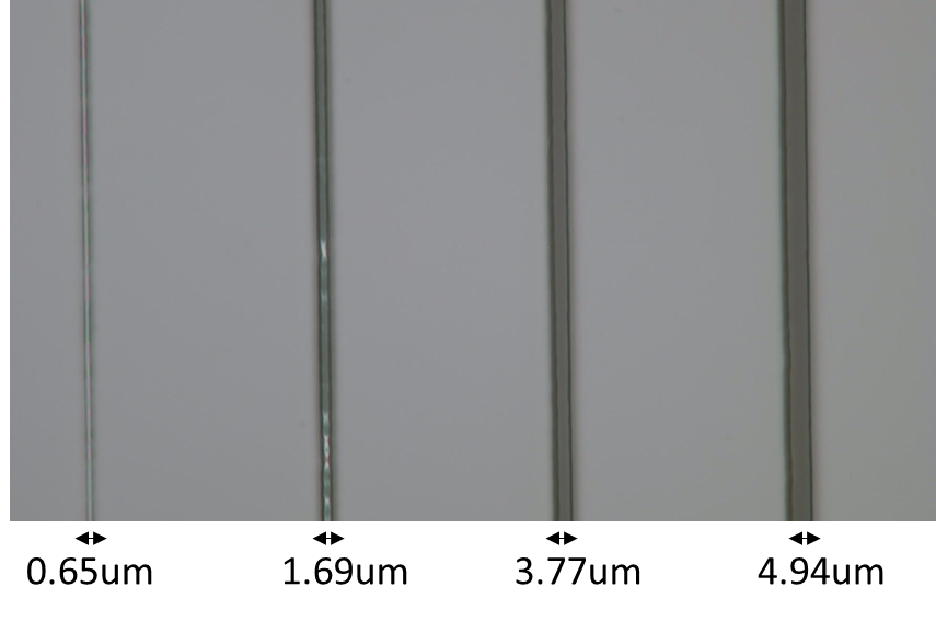
Employing a 50x objective lens with an NA of 0.75 and AZ1512 resist allows for high-resolution features by shrinking the photomask pattern down. The size reduction isn't 50x of the mask designs, likely due to diffraction enlarging the size of the mask, augmenting the image size before it reaches the objective lens. In this instance, a reduction of ~20x was achieved, producing features as small as 0.65 microns from a printed feature measuring 12.7 microns. If further reduction is desired, numerous optimizations and tricks can be employed. Initially, smaller mask features can be utilized. However, according to the Rayleigh resolution equation, with an NA of 0.75, a wavelength of 440 nm, and a k1 of 0.8, the limit may be ~469 nm. This initial work utilized a darkfield mask; alternatively, a clearfield mask with an overexposure can achieve sub-wavelength feature sizes at the expense of feature pitch. Other options include swapping to a smaller wavelength light source to increase resolution, changing the photoresist, or using a higher magnification objective lens at the expense of exposure field size, or increasing the NA of the lenses, among others.
Future plans for this system include homebrew transistor fabrication and research on wide band-gap materials.