Masks
1. Diffusion/LOCOS
2. Buried contact cut
3. Poly etch
4. Via etch
5. Metal etch
6. Contact cut

Possible Process Flow
1. Deposit Si3N4/Etch
2. Grow LOCOS oxide
3. Strip Si3N4 in hot phos
4. Grow gate oxide
5. Buried contact etch of oxide
6. CVD deposit poly
7. Poly Etch
8. Ion impact S/D and Gate
9. Drive in/activate implant
10. Phos spin on glass (SOG)
11. Etch vias through SOG
12. Deposit aluminum
13. Etch aluminum
14. Phos SOG
15. Contact cut etch
16. Wire bond
Reverse Engineering Semiconductor History
Examination and characterization of seminal semiconductor devices including point-contact diodes, the pioneering Intel 4004 microprocessor, and the inaugural planar transistor (2N1613)
The journey of semiconductor technology commenced at Bell Labs in 1947 with the inception of the transistor. Over the years, technology has morphed, often embracing varied processes and automated operations, which, while simplifying tasks to a mere button press, veil the intricate nature of these operations. The engineering prowess behind early devices often fades into oblivion over time. On the 75th anniversary of the transistor, IEEE discussed how the workings of the first transistor remain enshrouded in mystery today: https://spectrum.ieee.org/transistor-history. I find these pioneering devices fascinating to study for both historical appreciation and for how unconventional approaches from the past can provide insights into resolving contemporary challenges in the semiconductor realm.
The earliest semiconductor devices were cat-whisker diodes, utilizing Lead Sulfide, Silicon Carbide, and Silicon crystals with a fine metal wire in contact with the surface. These primitive diodes found applications in early radio work, comprising an antenna, tuning coil, diode for AC radio signal to DC conversion, and headphones for the listener. The cat-whisker diode essentially represented a basic Schottky contact between the metal and the semiconductor. Due to quality inconsistencies, operators needed to probe various crystal spots to find a sufficiently good contact point.
Reflecting on this history, I procured a Silicon cat-whisker diode and conducted a characterization using my HP4145 semiconductor parameter analyzer. The probing and electrical testing yielded divergent outcomes, with some areas behaving like a ~5 kohm resistor, while others exhibited Schottky performance. The favorable areas displayed a turn-on of ~0.3 V, characteristic of a Schottky contact, albeit in series with a parasitic resistor. This parasitic resistance contributed to subpar reverse bias performance and increased static for the user. Testing different "good" spots also revealed varying parasitic resistance values, aligning with early works on cat-whisker diodes and underscoring the revolutionary impact of the PN junction. Point-contact diodes, employing phosphorus-bronze wire for the cat-whisker and forming a thin PN junction through a high-current pulse, eventually supplanted the unreliable Schottky junctions of cat-whisker diodes, displaying superior reverse bias performance and stability.


Silicon cat-whisker diode (left), and I-V curves of good spot (right)
The Fairchild 2N1613 marked the debut of the planar transistor, symbolizing a technological leap courtesy of the planar process flow. The utilization of Silicon Dioxide as a masking and insulation medium, accompanied by multiple diffusions to craft a BJT in Silicon with top-only contacts, was groundbreaking. This approach mitigated the issue of particle-induced short circuits post-processing and introduced the concept of surface device fabrication, paving the way for microprocessors.
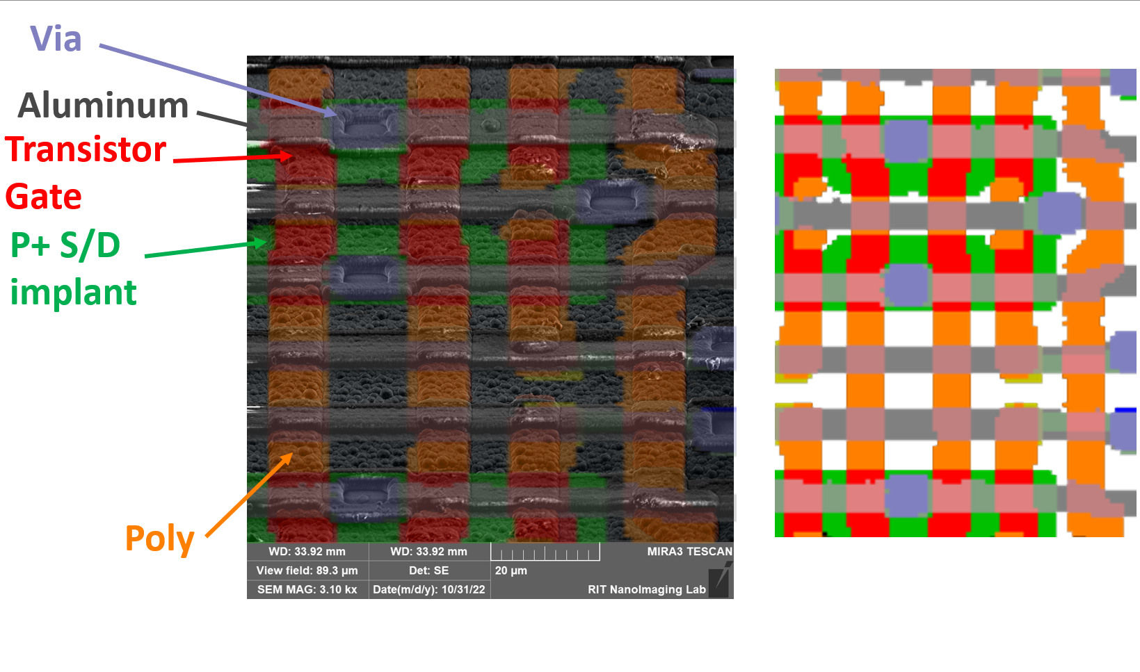
Intel pioneered the microprocessor realm with the Intel 4004, initially conceived for calculator applications to economize by consolidating eight chips into one. I acquired an Intel 4004 die and embarked on an exploration of its early history through die analysis. Significant efforts by others have preserved and digitized the 4004 mask set, aiding my analysis. SEM images of the index registers correlated with the mask levels, shedding light on the structure. The top layer revealed overserved Aluminum lines over the uneven spin-on-glass spacer oxide, beneath which lay the polysilicon gate lines and then the LOCOS oxide ridge, followed by the active device layers.


Intel 4004 Chip (left), and mask layout and false color SEM taken (right)
Zooming further disclosed more structural details, with a perfect overlay of the mask revealing two PMOS transistors in series as part of a cross-coupled inverter to store a single bit of data in the index register, one side connected to Vdd and the other to ground. A cross-section further showcased the transistors and the position of the buried gates, with gate lengths measuring ~5 microns.
Another cross-section along the gate unveiled the characteristic LOCOS "bird's-beak" formation. LOCOS, or LOCal Oxidation of Silicon, was an erstwhile technique for transistor isolation, now supplanted by shallow trench isolation or Silicon on insulator. Although abundant work exists on the operation of the 4004, discourse on its fabrication is scant. Below, I've delineated the mask levels and probable process flow.


SEM and FIB of PMOS cross-coupled inverter (left), and FIB of LOCOS isolation of PMOS wells (right)
Analyzing the process steps from these older technologies not only preserves the history of these devices but might also unearth forgotten techniques that could be pertinent today. I aim to continue exploring different historical semiconductor devices for analysis and preservation.